Achievements in next-generation 원탑토토 reliability technology through Hanyang University–SK hynix industry-university collaboration
Precisely measuring 원탑토토 interface adhesion using lasers
“We will continue to advance convergence between mechanical engineering and 원탑토토s”
A research team led by Professors Kim Hak-sung and Lee Seung-hwan (both from the School of Mechanical Engineering at Hanyang University) has developed a technology to precisely measure semiconductor interface adhesion in collaboration with SK hynix. This study quantified the microscopic interface adhesion inside semiconductors—previously difficult to measure—using a laser spallation technique, providing a foundation for enhanced reliability and quality in next-generation semiconductor processes.
Interface adhesion: a key factor in 원탑토토 reliability
Semiconductor products consist of complex structures with hundreds of ultra-thin stacked layers. Therefore, interface adhesion between each material serves as a crucial reliability indicator to prevent delamination and defects during long-term use. Professor Kim explained, “If an interface with weak adhesion delaminates during processing or usage, it can lead to failure of the entire product. Interface adhesion is critical not only for performance but also for product lifespan.”
Traditional methods for measuring interface adhesion rely on mechanical techniques applicable only to simple structures, which limits their effectiveness in delicate and complex semiconductor structures. Professor Kim explained, “Existing methods involve physically pulling apart two materials, but the internal semiconductor structure is small and fragile.” Professor Lee added, “In the semiconductor field, processes had to proceed without accurate interface data, which was like sailing with one eye closed.”
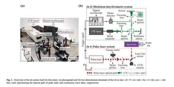
Realizing precise measurements with laser spallation
The core of this research is the laser spallation technique. This method involves irradiating the back of a silicon wafer with a laser to generate a compressive wave, which propagates through the silicon and induces tensile stress at the thin film interface to separate it. Professor Kim described, “Simply put, it measures how much resistance the front surface can offer when force is applied from behind. This process enables quantification of interface adhesion.”
Using the laser spallation technique, the team demonstrated the excellent adhesion strength of silicon oxide films formed via plasma-enhanced chemical vapor deposition (PECVD). Professor Lee commented, “There has long been speculation that adhesion strength varies depending on how the interface is formed, but few studies had quantified this. Our research is significant because it provides numerical evidence of interface adhesion strength.”
Achieved through close industry-university collaboration
This achievement was made possible through over ten years of close collaboration between Hanyang University and SK hynix. Professor Kim stated, “Laser spallation requires a deep understanding of both laser technology and mechanical analysis. This challenging research goal was achieved through long-standing trust and collaboration with SK hynix.”
Regarding future prospects, Professor Kim added, “Laser spallation technology is applicable to all types of interfaces, and we plan to expand its application to advanced packaging and glass substrates. SK hynix is also considering using it as a practical tool for process optimization and product reliability.” Professor Lee emphasized, “As we can now verify interface reliability from the manufacturing stage, this technology will be widely useful throughout the semiconductor industry.”

The power of convergence: mechanical engineering meets 원탑토토s
This study is a representative example of mechanical engineering making a significant contribution to semiconductor technology, which has traditionally been seen as the domain of electrical and materials engineering. Professor Kim noted, “This achievement is an answer to how mechanical engineering can contribute to semiconductor technology. In an era where interdisciplinary convergence is a core competitive advantage, breaking down boundaries between fields is essential.”
Since 2022, Hanyang University has operated the Advanced Semiconductor Packaging Center, fostering active interdisciplinary research among professors from mechanical, electronic, electrical, physics, and materials engineering. Professor Kim, who leads the center, stated, “We will continue active convergence research in the semiconductor field through Hanyang University’s infrastructure and industry-university collaboration.” Professor Lee added, “We will strive to continuously contribute to the development of core technologies that lead the global semiconductor industry.”
 '한양위키' 키워드 보기